Sivers Semiconductors Advances LiDAR Chip Production with CW DFB Lasers, $53–138 M Revenue Potential
The global LiDAR market is entering a phase of rapid commercialization. The driver is straightforward: automotive ADAS mandates are tightening worldwide, robotaxi fleets are demanding higher‑resolution ranging, and non‑automotive segments—industrial robotics, warehouse automation, and agricultural machinery—are adopting solid‑state sensing at an accelerating clip. Beneath the headline‑ grabbing shipment figures, the real bottleneck has been the supply of reliable, high‑power continuous‑wave distributed‑feedback (CW DFB) lasers and the optical amplifiers that keep them stable. In October 2026, Sivers Semiconductors announced that its strategic LiDAR customer has moved from design‑win to production, initiating first production orders that will begin shipping in Q4 2026 and scale through 2027. The program carries an estimated cumulative revenue potential of USD 53 million to USD 138 million over the customer’s product lifecycle, which places it among the largest single photonics wins disclosed by a specialty semiconductor company this year.
The Design‑Win Program: A Multi‑Year Revenue Opportunity
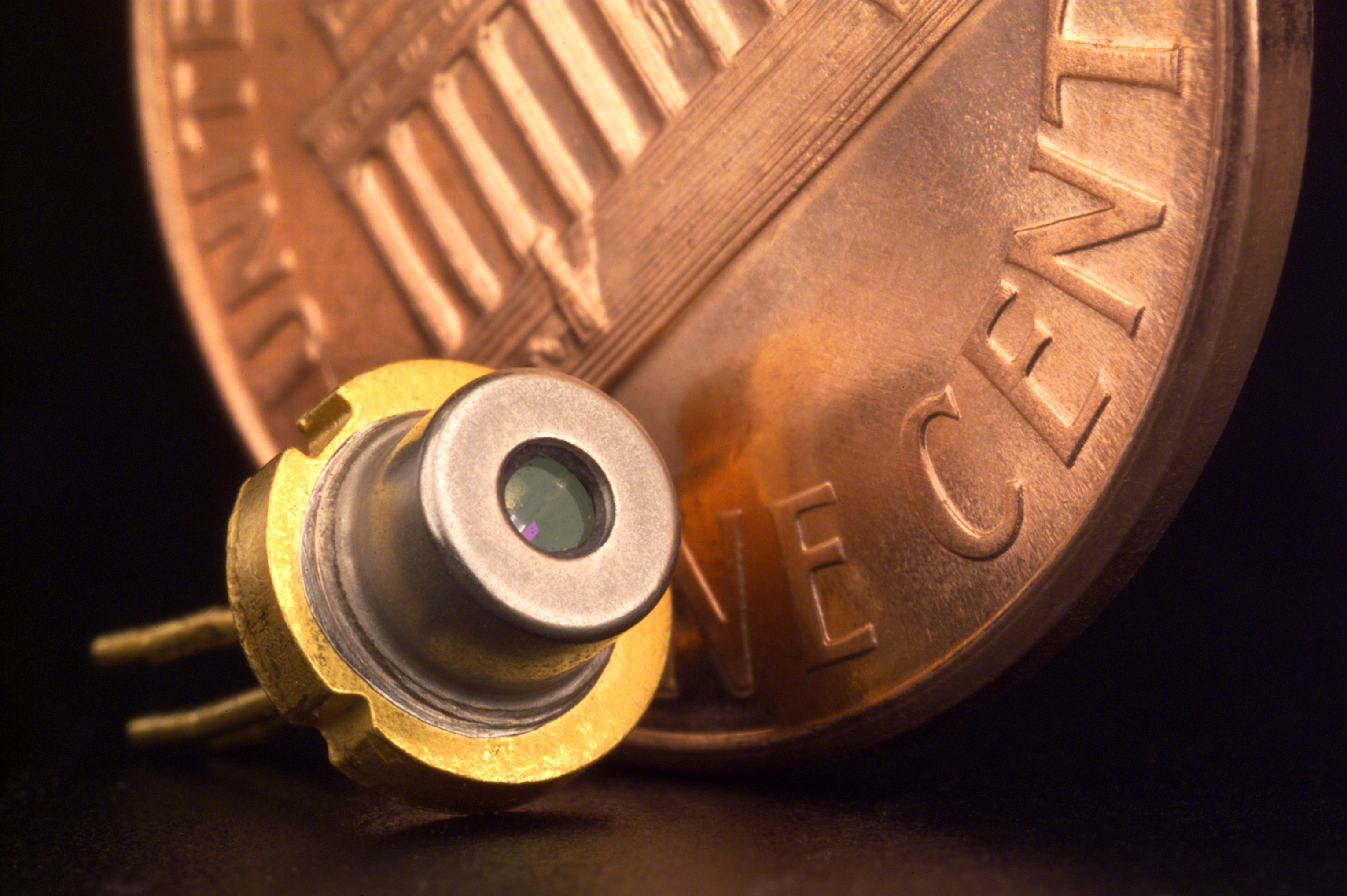
Sivers’ photonics business supplies the CW DFB lasers and optical amplifiers that form the ranging core of the customer’s LiDAR hardware. As Alex McCann, Managing Director of Sivers’ photonics business, stated in the company’s 20 October 2026 press release, “We are pleased to see this strategic program advance from design‑win to production, with our customer placing first production orders. This key milestone reflects confidence in our technology, our production facility and its reliability to meet the customer’s requirements for volume production. As the program scales, we expect rolling production orders placed to lead times, in line with our customer’s multi‑year production forecasts.” The program was originally disclosed in March 2026, when Sivers first signalled that an undisclosed Tier‑1 customer had completed the design phase and committed to qualifying Sivers’ InP‑based laser architecture for automotive‑grade production.
The laser modules are built on indium‑phosphide (InP) DFB architecture, chosen for its narrow linewidth—typically below 100 kHz—and its temperature stability across the −40 °C to +125 °C range that automotive qualification demands. These attributes matter because LiDAR ranging accuracy degrades quickly if the optical frequency drifts; a DFB laser that holds its wavelength under thermal stress directly translates into centimeter‑level precision at 200 meter ranges. Sivers’ facility in Kista, Sweden, was audited by the customer against IATF 16949 and ISO‑26262 ASIL‑B standards before the production‑order decision was taken, and the company has said the qualification included endurance runs of more than 2,000 accelerated‑aging hours. The production ramp is expected to be staged: low‑rate initial production in late 2026 feeding into higher‑volume builds in 2027, with the rolling order cadence mirroring the customer’s vehicle‑build forecasts.
CW DFB Lasers and the Photonics Supply Chain
The semiconductor story here is as much about supply‑chain reliability as it is about raw performance. CW DFB lasers are not commoditized commodities; they require specialized epitaxy on InP wafers, sub‑micron grating patterning, and facet‑coating processes that few fabs master at volume. Sivers’ competitive advantage, according to its March briefing quoted by Semiconductor Today, rests on a vertically integrated photonics line that handles wafer growth through final test, a combination that lets the company hold yields above 75 percent on the highest‑power variants. The company also supplies RF beam‑former ICs and lasers for AI data‑center and SATCOM applications, giving it a cross‑segment view of where optical‑source demand is heading.
A second dimension of supply‑chain risk is the availability of high‑purity InP substrates. Global InP wafer capacity is concentrated among a small number of epitaxy houses, and lead times stretched to more than 18 weeks in early 2026 as AI‑datacenter co‑packaged optics projects competed with automotive LiDAR programs for the same substrate lots. Sivers mitigated this by securing multi‑quarter substrate allocations ahead of the March disclosure, a move that the PhotonCap newsletter later linked to the program’s ability to commit to the production timeline without a substrate bottleneck.

Market Dynamics: Yole, Gasgoo, and the Dual Automotive–Non‑Automotive Expansion
Yole Group projects that the global automotive LiDAR market will expand from USD 861 million in 2024 to USD 3.8 billion by 2030, a compound annual growth rate (CAGR) of 28 percent. In a separate 2026 report, Yole estimated the broader ADAS market will reach USD 66 billion by 2026, figures that give context to why a single photonics design win can justify an $138 million lifecycle valuation. The growth is not purely automotive, however. A July roundup by Gasgoo found that Seyond’s LiDAR shipments surged to roughly 271,100 units in Q2 2026, a 385 percent year‑on‑year increase, while total Chinese passenger‑vehicle LiDAR installations topped 1.3 million units in the first four months of 2026.
The market hierarchy that has emerged is worth examining because it frames the playing field that Sivers is entering. Hesai leads the automotive primary‑LiDAR segment with an estimated 43 percent global market share, while Huawei follows with a growing footprint through its Harmony Intelligent Mobility Alliance and an 896‑line dual‑optical‑path sensor that debuted on the Maextro S800 and AITO M9 in March 2026. RoboSense, third globally, reported that its Q1 robotics‑LiDAR sales jumped 1,458 percent year‑on‑year and now account for about 56 percent of its total volume. The implication is twofold: high‑end automotive volumes are being won by a duopoly with deep OEM ties, while the long tail of demand—robotics, logistics, and industrial autonomy—is fragmenting the addressable base in precisely the way a specialty supplier like Sivers hopes to profit from.
Position in the Semiconductor Photonics Ecosystem
For investors and analysts, the Sivers win is a reminder that the semiconductor value chain is splintering at the component level. Yahoo Finance re‑capped the announcement three days after release, noting the $53 M–$138 M figure and highlighting the cadence of rolling orders as the key revenue‑visibility signal. Market‑microstructure coverage from Morningstar and PR Newswire framed the decision as confirmation of a “previously disclosed design‑win moving toward production,” effectively turning a forward‑looking disclosure into a revenue‑recognized milestone.
The March 2026 disclosure had already hinted at the revenue range, but the October production‑order trigger is what moves the program from the “pipeline” column to the “recognized backlog” column on Sivers’ books. That matters because Sivers’ fiscal calendar treats multi‑year photonics contracts as percentage‑of‑completion revenue, meaning quarterly earnings visibility extends well into 2027. For a company with a market capitalization just above $130 million (per Silicon Matter’s March 2026 profile), a single $138 million tailwind is material to its valuation narrative.
Risks and Forward Watchpoints
Three risks dominate the second‑half trajectory. The first is InP substrate availability: if the leading epitaxy houses hit yield setbacks, wafer lead times could extend past the 18‑week buffer that Sivers has described. The second is the cadence of the customer’s vehicle‑build schedule: the production orders described by Sivers are rolling, which means they are tied to end‑customer demand forecasts that can shift under inventory cycles. The third, and perhaps the most structural, is competitive entry: established optical component suppliers such as II‑VI (now Coherent) and new fabless entrants have been qualifying their own DFB architectures for the same Tier‑1 slots, and their scale advantages could pressure average selling prices if Sivers’ yield edge erodes.
A useful forward indicator is the timeline of Sivers’ own disclosures. The March 2026 announcement disclosed the design win and the revenue range but gave no shipment schedule; the October 2026 trigger disclosed the first production orders and the Q4 start‑of‑shipments window. The next checkpoint is likely to be Sivers’ fiscal Q4 results, expected in early 2027, where the company may quantify the first tranche of recognized revenue from the program.
Conclusion
Sivers Semiconductors’ transition from design‑win to production is a concrete step toward commercializing high‑power CW DFB lasers for a market that is shifting from prototype to volume in real time. With a projected revenue potential of $53 M–$138 M, staged production starting in Q4 2026, and a market backdrop in which Yole sees a 28 percent CAGR and Gasgoo sees quarter‑on‑quarter shipment growth of 385 percent, the program sits at the intersection of advancing semiconductor photonics and the accelerating adoption of solid‑state ranging technologies. As automotive OEMs finalize their Level‑3 and Level‑4 platform schedules and as robotics manufacturers move beyond the pilot stage, the demand for reliable, automotive‑grade laser sources is set to intensify. That dynamic positions Sivers’ photonics portfolio—notably its InP DFB architecture—as a critical enabler in the semiconductor supply chain for the autonomous‑driving decade ahead.
Sources
- Sivers Semiconductors press release, 20 October 2026 – “Strategic LiDAR Customer Initiates Production Orders with Sivers Semiconductors”
- Yahoo Finance re‑print of the same announcement (23 Oct 2026)
- Morningstar / PR Newswire coverage (23 Oct 2026)
- Compound Semiconductor, “Sivers to begin production for key LiDAR customer” (20 Oct 2026)
- Semiconductor Today, “Strategic LiDAR customer initiates production orders with Sivers” (20 Oct 2026)
- Gasgoo, “LiDAR Growth Accelerates as Non‑Automotive Markets Take Off” (7 July 2026)
- Yole Group, “From sensors to software: ADAS market accelerates toward $66 billion” (27 May 2026)