Samsung Lands $200 Billion Broadcom Chip Deal in AI Infrastructure Push
Samsung Electronics has secured a deal worth more than $200 billion to supply memory and foundry chips to Broadcom over the next five years, in what stands as one of the largest semiconductor supply agreements in the industry's history.
The memorandum of understanding was signed at the AI Summit in San Francisco, with Samsung Foundry President Jinman Han and Broadcom CEO Hock Tan both on hand. The pact runs through 2030 and covers High Bandwidth Memory (HBM) for Broadcom's next-generation AI accelerators, as well as 2-nanometer and below process technologies for wireless broadband communications, networking, and AI infrastructure products.
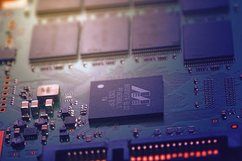
"AI is creating unprecedented demand for tightly integrated semiconductor technologies spanning memory, logic and advanced packaging," said Young Hyun Jun, Vice Chairman and CEO of Samsung's Device Solutions division, in a statement. Samsung is aiming to use its unique position as a company that handles memory, foundry, and advanced packaging under one roof to win more such deals.
Charlie Kawwas, President of Broadcom's Semiconductor Solutions Group, said the collaboration would help the company scale its AI infrastructure amid a rapid buildout. Broadcom designs custom AI accelerators for hyperscalers including Google and Meta, and has been one of the biggest beneficiaries of the AI infrastructure spending wave, with AI-related revenue tripling year-over-year.
A Closer Look at the Deal
The agreement breaks down into two main pillars. On the memory side, Samsung will supply industry-leading HBM solutions to support Broadcom's AI accelerator roadmaps. The memory chips are a critical bottleneck in AI system performance, as large language models need fast access to massive datasets during training and inference.
In foundry, Samsung's 2nm Gate-All-Around (GAA) process will be used to manufacture Broadcom's chips. Samsung has been racing with TSMC to commercialize 2nm production, and this deal gives it a marquee customer for what it bills as its most advanced logic process. Broadcom's wireless broadband and networking chips require the power efficiency and density that 2nm promises.
The MOU also covers advanced packaging technologies, an increasingly important piece of the semiconductor puzzle. As chip designs grow more complex, stitching together multiple dies into a single package—known as heterogeneous integration—has become essential for AI workloads. The global advanced packaging market is expected to reach $78 billion by 2030, according to industry estimates.
The deal comes at a time when semiconductor companies are racing to lock in supply agreements. The global chip shortage of 2021–2023 taught hyperscalers and networking firms that spot-market procurement of leading-edge chips carries enormous risk. Long-term pacts like this one give both sides predictability: Samsung gets a committed buyer for its 2nm output, and Broadcom gets guaranteed supply at a time when foundry capacity is stretched thin by AI demand.
Why This Deal Matters
The $200 billion figure underscores how quickly AI infrastructure spending is reshaping the semiconductor supply chain. Broadcom expects to deploy tens of billions of dollars in custom AI silicon over the next five years, and locking in foundry and memory capacity with Samsung ensures it won't be caught short as demand surges.
Samsung, for its part, needs the win. The company has been trying to grow its foundry market share against TSMC, which controls roughly 70% of the global contract chipmaking market. Landing Broadcom as a 2nm anchor customer provides a powerful reference for other potential clients. Samsung's foundry business has been investing heavily in its GAA technology, which it positions as a more power-efficient alternative to TSMC's FinFlex approach.
Industry analysts say the deal also reflects a broader trend: hyperscaler demand for custom silicon is pushing chip designers and foundries into longer-term, higher-value partnerships. Broadcom's AI revenue has tripled year-over-year, fueled by TPU-like custom accelerators it builds for cloud providers. The Samsung agreement secures the supply chain for that growth.
Samsung's Memory Strength
On the memory side, Samsung is the world's largest maker of DRAM and NAND flash. Its HBM3E and upcoming HBM4 memory modules are designed specifically for AI accelerators, stacking multiple DRAM dies vertically to achieve ultra-high bandwidth. Broadcom's next-generation accelerators will rely on these modules to feed data to compute cores without stalling.
Samsung also announced earlier this year that it had begun mass production of what it calls the industry's highest-capacity HBM3E memory, with 36 GB per stack. Analysts expect HBM demand to grow more than 40% annually through 2030 as AI models grow larger and require more memory bandwidth.
There are also questions about whether the broader memory market can keep up. NAND and DRAM prices surged in 2025 and early 2026 as AI server buildout consumed an ever-larger share of output. Some analysts have warned that memory price inflation could squeeze non-AI segments of the electronics industry, an effect Sravan Kundojjala of SemiAnalysis called "the memory boom squeezing TSMC's non-AI business." The same pressure applies to Samsung, which must balance HBM profitability against its broader memory portfolio.
The Broader AI Chip Sector
The Samsung-Broadcom deal comes amid intense activity across the semiconductor sector. Intel recently announced a collaboration with Lens Technology to explore glass-based advanced packaging substrates for the AI era. The collaboration combines Intel's advanced packaging R&D with Lens Technology's materials engineering, targeting new manufacturing processes that can scale to meet AI chip demands.
Intel announced the collaboration with Lens Technology on July 28. Lip-Bu Tan said the work would "explore potential areas of cooperation in critical manufacturing processes to scale the adoption of advanced semiconductor packaging." Glass substrates promise better thermal performance and dimensional stability compared to traditional organic materials, which could matter as chip packages grow larger and more complex.
TSMC, for its part, reported a 77% jump in second-quarter profit in mid-July and announced an additional $100 billion investment in its Arizona fab complex, bringing total planned US investment to $265 billion, as CNBC reported. The Taiwanese foundry giant said "AI-related demand is extremely strong," according to Chairman C.C. Wei. TSMC's Q2 revenue hit NT$1.27 trillion, a 36% year-over-year jump, with high-performance computing accounting for 66% of total revenue.
Nvidia and Amkor Technology also struck a $1.5 billion chip packaging deal, underscoring the industry-wide race to expand packaging capacity—often called the "back-end" bottleneck—as front-end fabrication advances at breakneck speed.
The China Factor
The semiconductor industry is also watching developments in China closely. Reports emerged on July 27 that a state-backed Chinese company had started mass-producing its own deep ultraviolet (DUV) lithography machines, sending AI chip stocks into a brief selloff. While the machines are not expected to compete with ASML's extreme ultraviolet (EUV) tools for leading-edge nodes, they could give Chinese foundries like SMIC more capacity for 28nm and 14nm-class production, potentially flooding the mature-node market.
The news triggered a 3–5% drop in several semiconductor stocks before the market recovered the same day. It also reignited debate about whether export controls on Dutch and Japanese lithography tools are slowing China's chip ambitions as much as policymakers in Washington and Brussels had hoped.
What's Next
Samsung is expected to begin 2nm risk production in early 2027, with the Broadcom chips likely entering volume production later that year. The two companies said the collaboration could also extend to other areas, including research on next-generation memory architectures and co-packaged optics for data center interconnects.
For Broadcom, the deal cements a multi-sourcing strategy for foundry capacity. The company already works with TSMC on some products, and adding Samsung as a second source for leading-edge chips gives it supply chain flexibility—an increasingly important consideration as geopolitical risks shadow the Taiwan-centered semiconductor industry.
Already Asia's most valuable technology company, Samsung Electronics is making a calculated bet that its integrated device manufacturer model—covering design, memory, foundry, and packaging—gives it a unique edge in an industry where the barriers between chip types are blurring. The Broadcom deal is its strongest evidence yet that the strategy is working.
Samsung is also expanding its production footprint. The company broke ground on a new foundry line in Taylor, Texas, earlier this year, with initial production targeted for late 2027. That facility is expected to manufacture 2nm and 3nm chips for US customers, including Broadcom and other AI-focused firms that prefer onshore fabrication.
On the memory side, Samsung has been pushing HBM capacity aggressively. The company invested roughly $20 billion in memory expansion in 2026 alone, with most of that going toward HBM3E and HBM4 production lines. SK Hynix, Samsung's main rival in HBM, has also announced major capacity additions, raising questions about whether the market could face oversupply if AI demand growth slows.
For more semiconductor industry coverage, check out our Semiconductors category and AI coverage.