Taiwan Foundries and Global Equipment Demand Drive 23% Spike in Semiconductor Billings
The world's leading chipmakers are racing to lock in capacity for AI workloads as the global semiconductor equipment market logged its strongest quarterly expansion in more than a year. South Korea remains the dominant anchor of the global supply chain, and Taiwan's foundries are absorbing more of the investment than any other country.

Taiwan fabs accelerate fivefold expansion to match AI chip demand
Taiwan Semiconductor Manufacturing Co. (TSMC) said it is ramping up capacity fivefold this year even though the industry giant can barely keep pace with the surge in AI chip orders. The comments, published on September 3, highlight how server GPUs and accelerator ASICs are straining existing supply lines as hyperscalers triple down on inference clusters. TSMC did not name customers, but the focus on AI workloads aligns with its recent reported guidance that data-center logic chips now account for more than half of its revenue.
The speed of expansion is unusual for a company whose 3nm production engines have only recently begun moving into volume. TSMC's move signals that long-term contracts with cloud providers and large language model builders are locking in capacity months in advance, leaving less elbow room for opportunistic bidding from fabless clients in markets like automotive or consumer IoT. As a result, the foundry is assuming a more aggressive wafers-per-month profile than it has kept in internal forecasts as recently as H1 2026.
The fivefold figure likely refers to the rate of capital equipment installations at TSMC's major Arizona, Kumamoto, and Kaohsiung fabs. Arizona Phase 2 has been running pilot lines for months, while Phase 3 is already deep in structural construction. On the southern Taiwan coast, TSMC's advanced packaging capacity is growing alongside its mainstream front-end foundry lines, an important signal that chiplet designs and high-bandwidth memory stacking are scaling in lockstep with logic density gains.
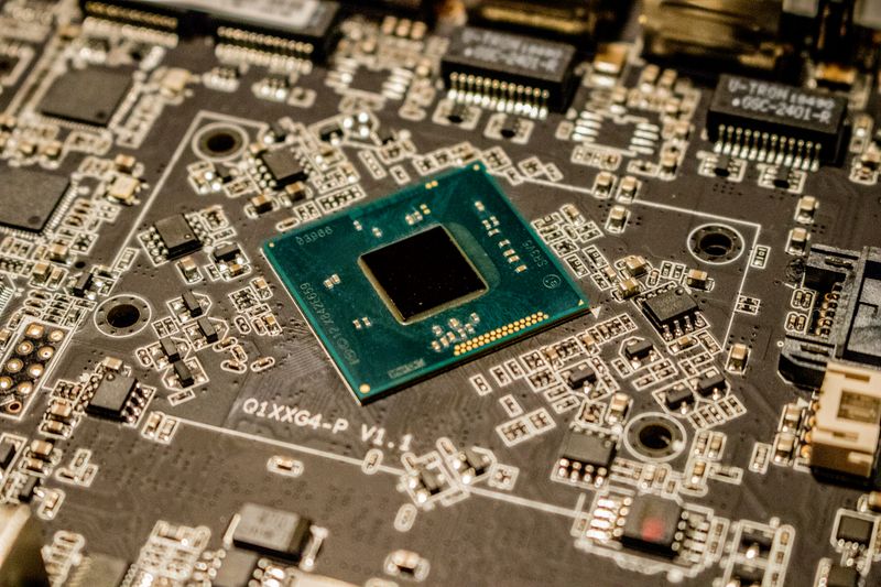
Equipment spending jumps 23% on AI-driven fab buildouts
Investors took note when the global semiconductor equipment billings report showed a 23% year-on-year rise in the second quarter of 2026. Total billings, collected by SEMI and other industry trackers, reached US$40.53 billion, a level last seen in late 2024 and fully powered by demand for AI-capable factories. The bulk of the incremental spend is on lithography, deposition, and etch tools designed for nodes below 5nm, all of which are essential for building chips that can cope with the power and throughput constraints of modern training and inference clusters.
Revenue gains are not evenly distributed. Systems makers that dominate deep ultraviolet (DUV) and extreme ultraviolet (EUV) lithography, as well as advanced packaging, are seeing the biggest jumps in bookings. The pattern is consistent with what analysts have been calling the "AI fab premium" — a persistent pricing and backlog pressure on the most advanced equipment required to meet country-independent capacity commitments with hyperscalers.
South Korea, home to Samsung Foundry and SK Hynix, remained the top equipment buyer during the quarter, followed closely by Taiwan and then mainland China. The continued high ranking of China is particularly notable given export controls on certain advanced tools; Chinese fabs have been snapping up mature-node and DUV equipment at a pace that keeps regional equipment vendors well supplied. In mature nodes used for power management ICs and microcontrollers, Chinese fabs are building more capacity than any other country in the world, a shift that will reshape pricing dynamics for legacy semiconductors through at least the end of the decade.
ASML leads High-NA EUV buildup amid foundry partnerships
ASML's next-generation high-numerical-aperture EUV tools are gathering momentum after TSMC, Samsung Electronics, and Intel Foundry expanded collaboration in late August and early September. The trio signed joint statements backing ASML's High-NA EUV program, which uses a 0.55 NA lens system to deliver patterns more than twice as dense as current EUV platforms. The new systems are not ready for mass production, but the tripartite commitment means the machines should enter key customer fabs within the next 12 to 18 months.
Samsung will use the newest High-NA EUV systems for memory chips starting in 2028, while TSMC has indicated it will follow for logic chips in 2030. Intel Foundry has not specified its integration timeline, but the partnerships underscore how nothing short of High-NA EUV and related EUV variants can meet the pattern-density requirements of power-savvy, speed-critical AI accelerators without advancing node pitches beyond 2nm. ASML's leadership in this space means the company will likely maintain a near-monopoly position on EUV production through at least 2027, though analysts note that a single political disruption in the Netherlands could rapidly reorder the global supply chain.
The tripartite backing is not purely altruistic. Each foundry gains a share of ASML's High-NA development roadmap data, giving them a first-mover advantage in optimizing their next-generation process flows. For ASML, having three major customers underwrite the R&D reduces the financial risk of deploying what is expected to be a EUR150 million-plus per tool platform. The broader implications are straightforward: if High-NA EUV does deliver as projected, the next two node generations of chips from TSMC, Samsung, and Intel will be denser, faster, and more energy-efficient than anything on the current roadmap — a shift that matters most for the power-hungry data-center chip market.
What this means for device makers and downstream industries
For fabless chip designers, the expanding capacity and advanced-node choices mean access to more 3nm and 2nm capacity — but at premium pricing and allocation quotas that favor long-term AI customers. For device makers, including smartphone OEMs, automotive suppliers, and cluster manufacturers, a tighter supply picture could mean longer lead times and higher incremental costs. On the positive side, more invested fabs reduce the odds of capacity bottlenecks limiting how quickly AI-capable devices can be deployed globally.
The current expansion wave is not a guarantee that the semiconductor cycle will stay red-hot. Equipment consumption typically slows as fabs complete construction, and trade tensions and domestic policy shifts can cut into margins. Still, the industry's hedging behavior — capitalizing on every dollar of available funding now, while firms with deeper pockets battle over scarce capacity — suggests that production footprints will be reshaped for the duration of the current AI boom.
One notable casualty of the current cycle is the relative neglect of mature-node capacity expansion outside China. Power management ICs, analog chips, and microcontrollers still make up a substantial portion of the global semiconductor market by unit volume, and the lack of new investment in that segment could produce localized shortages in automotive and industrial supply chains within the next 18 to 24 months. For readers tracking the broader hardware ecosystem, this is a case where the AI-driven capacity boom may mask real vulnerabilities in the non-AI chip supply chain.