Samsung Holds Back High-NA EUV Mass Production as Foundry Unit Struggles With Costs
By Tech Desk | August 27, 2026
ASML Holding NV has already moved its next-generation High-NA extreme ultraviolet (EUV) lithography systems into volume production for Intel Corp's 18A Panther Lake processors, yet Samsung Electronics Co Ltd has reportedly kept the same machines on the sidelines. The Korean chipmaker installed two High-NA EUV systems in its Pyeongtaek campus but has not ramped them for mass output, according to industry sources. The move reflects a hard-nosed cost calculation rather than a technical shortfall, and it lays bare how differently the three leading-edge foundries are playing the sub-2nm game.
ASML ships the tool, but only some customers run it
The High-NA EUV — short for high numerical aperture EUV — is the biggest leap in lithography since the first insertion of EUV in the late 2010s. With a numerical aperture of 0.33, the platform can print features as small as 8nm and lets fabs skip the double-patterning steps that older EUV needed at the most aggressive nodes. ASML delivered the initial High-NA EUV systems in 2023, and by mid-2026 Intel had woven the tool into its high-volume flow for client processors. Other buyers have been more cautious.
Samsung's case is instructive. The company took delivery of two High-NA EUV scanners but has not yet pushed them into full-rate manufacturing. Chosun Ilbo reported that observers inside the supply chain read the restraint as a financial decision: Samsung wants to avoid pouring more capital into a foundry business that has already bled red ink for several quarters. The logic is simple. Each system carries a price north of $350 million, and bringing one online means not just the tool itself but cleanroom space, process recipes, metrology, and months of yield learning. When the order book is thin, that math is hard to justify.
Three foundries, three very different playbooks
Three names dominate the leading-edge race: TSMC, Samsung Foundry, and Intel Foundry. Their models could hardly be more different. TSMC, the pure-play foundry leader, spreads the cost of new equipment across a huge and diverse customer base, which lets it adopt early without betting its own product line. Intel, once purely internal, now runs a foundry arm and has leaned into High-NA EUV as a wedge to win external clients and to anchor its own 18A and follow-on nodes. Samsung sits in the middle — a vertically integrated giant whose chip unit competes with its own components business for capital.
That middle position shapes every spending choice. Samsung's semiconductor division has posted operating losses in recent quarters, and its foundry side has ceded share to TSMC at the most advanced nodes. Under those conditions, a $350 million-plus scanner that may sit partially idle looks like a liability rather than a weapon. Intel can absorb the cost because it feeds its own roadmaps; TSMC can spread it across dozens of design winners. Samsung has neither cushion in equal measure.
The tool is ready; the business case is not
On the engineering side, readiness is not the blocker. ASML has said the High-NA platform hits new readiness milestones on a regular cadence, and Intel's demonstration of volume-capable 18A wafers shows the tool can do the job. Printing 8nm half-pitch without double patterning removes a whole layer of process complexity and cycle time. From a pure technology standpoint, the boxes work.
The harder question is return on capital. Process development, yield ramp, and equipment amortization all take time and money before a single paying wafer ships. For Samsung, the calculus weighs the performance edge of High-NA EUV against the immediate hit to free cash flow. Analysts note that the foundry unit's losses make any fresh capital outlay a board-level debate, not a routine line item. The issue is not whether the machine prints good patterns — it is whether the volume and margin follow fast enough to pay for it.
What the slowdown means for the supply chain
Uneven High-NA EUV adoption ripples through the whole chip ecosystem. Customers chasing the sharpest nodes will find capacity concentrated at Intel and, soon, TSMC, which is expected to follow Intel's lead within the next year or so. That concentration can tighten lead times and lift prices for the most advanced masks. ASML, for its part, has its early High-NA volume win with Intel and a clear second wave forming behind it. Samsung's pause leaves a temporary hole in third-party High-NA capacity, mainly affecting fabless firms that might have spread orders across three suppliers.
The High-NA story is also one chapter in a wider manufacturing shift. As classic transistor scaling gets more expensive, the industry is leaning on advanced packaging, backside power delivery, and new transistor shapes such as gate-all-around (GAA) to keep performance climbing. High-NA EUV sits alongside those techniques rather than replacing them. How fast any one company adopts it depends on its roadmap, its balance sheet, and the customers it needs to win.
Why the pause matters for Samsung's turnaround
Samsung's foundry business has been the weak link in an otherwise strong semiconductor group. Memory profits have rebounded on AI demand, but the logic side has lagged TSMC in both yield and customer trust at the leading edge. Holding off on High-NA EUV may protect cash now, yet it also risks a longer gap in the most advanced node race. Rivals are not waiting. Intel's 18A is in volume, and TSMC's N2 and A16 nodes are drawing design wins that could lock in multi-year commitments.
The bet Samsung appears to be making is that process maturity and customer confidence matter more than being first to a tool. If its 2nm-class yields improve and orders return, the deferred High-NA spend could be restarted without falling irrecoverably behind. If not, the pause may harden into a structural disadvantage. Either way, the decision shows how capital discipline and technology ambition pull a modern foundry in opposite directions.
A staggered rollout, not a shared starting line
Samsung's reported hold on High-NA EUV mass production shows the gap opening between what is technically possible and what is financially sensible in leading-edge chipmaking. Intel and TSMC are pushing ahead; Samsung is waiting for the business case to clear. As the sector drives past the 2nm mark, expect a staggered rollout instead of a synchronized one. For now, the High-NA front is led by Intel and TSMC, and Samsung's next move will be read as a signal for how the rest of the foundry field will pace its own capital spending.
Keywords: semiconductor, foundry, High-NA EUV, ASML, Intel, Samsung, lithography, 18A, Panther Lake, chip manufacturing, process technology
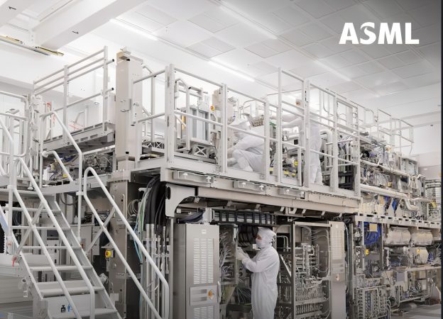
The High-NA EUV platform can print features as small as 8nm and removes the need for double patterning at the most aggressive nodes.
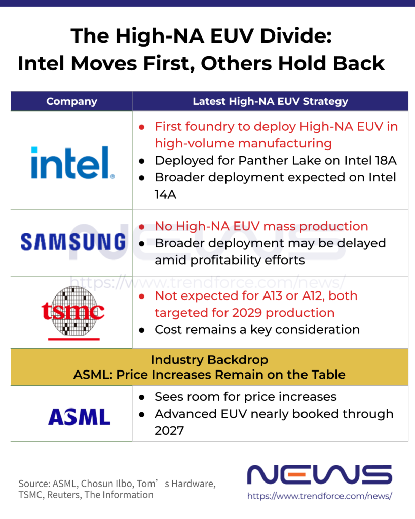
The High-NA EUV divide shows how differently the three leading foundries are pacing their tool deployments.
Related: Semiconductors coverage
ASML High-NA EUV readiness milestone
Additional details on the High-NA technology gap
Beyond the business considerations, there are also meaningful technical differences between how each foundry is using the High-NA EUV platform. Intel has spoken publicly about integrating the scanner with its backside power delivery architecture on 18A, a combination that could enable performance per watt gains beyond what earlier nodes achieved. TSMC has said its N2 node will employ High-NA EUV for critical layers only, reserving older EUV for less demanding patterns — a mixed-strategy approach that spreads risk and controls capital spend. Samsung, for its part, has been quietly advancing its own 2nm-class process development, which the company calls SF2, and industry sources suggest the firm may already have working test chips at that node even without High-NA EUV volume production. The existence of SF2 means Samsung is not standing still; its engineers are applying alternative methods — improved double patterning, triple patterning in select layers, and layout optimizations that push density higher without the most expensive tool in the ASML lineup. These alternative paths can deliver meaningful performance per watt improvements, even if they lack the headline-grabbing simplicity of a single-scanner solution. The trade-off is complexity: more masks, more alignment steps, and a steeper yield learning curve that can eat into the very margins Samsung is trying to protect with its capital restraint.