Samsung Flips AI Memory on Its Head: New zHBM Stack Sits Memory Right on Top of the Processor
Samsung Electronics pulled the lid off a memory architecture it says is the industry's first of its kind, and the whole pitch is about rearranging the hardware. The company showed concept models of something it calls zHBM at the Future Memory and Storage conference, known as FMS, in Santa Clara on Tuesday, and the core idea is deceptively simple: stop putting high-bandwidth memory next to the AI processor, and start stacking it directly on top.
Samsung says the design can deliver up to eight times the performance of HBM5, the current generation of high-bandwidth memory. It is no longer just talking about making the chips faster or the wires between them tighter. It is talking about changing the geometry of how memory and silicon talk to each other at all.
Yonhap, the Korean wire service, reported the unveiling on Wednesday and put the number on a next-generation interface system. Density goes up more than tenfold versus HBM5 thanks to wafer bonding, energy efficiency roughly triples, and thermal resistance drops by more than half. Those are the headline claims, straight from Samsung's announcement.
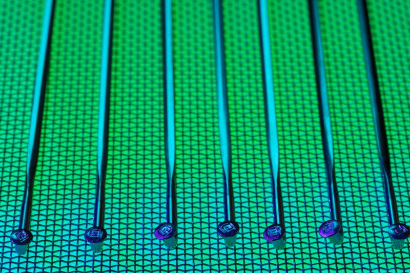
For context on what zHBM is competing against, it pays to recall what a typical HBM stack looks like today. A conventional high-bandwidth memory package is a tall column of DRAM dies stacked with through-silicon vias, sitting on an interposer next to the compute die. Every generation has added more layers and tightened the connections between them, and that has worked. HBM3e and HBM4 carry more bandwidth than their predecessors and the industry keeps paying a premium for them. The unstated problem is that the geometry has stayed flat. The memory climbs into the sky inside its own package, but it still sits on the board beside the processor, and the interface between the two is the real choke point.
That is the gap Samsung is trying to attack. zHBM does not just keep scaling the vertical stack; it repositions the whole assembly so the memory sits on top of the accelerator, above it rather than beside it. The company's materials describe memory density several times that of a conventional stack, big power savings, and better thermal behavior because the resistance that traps heat drops by more than half. Whether every one of those numbers survives contact with a real product is a question for later, but the intent is clear.
The bottleneck that will not move
Here is why the company is bothering. AI accelerators, from GPUs to the custom silicon now flooding data centers, spend most of their working life pushing data back and forth to memory. The processor is fast; the road between it and the memory is not. In a conventional HBM package, the memory dies sit beside the accelerator on the same plane, and every read or write has to travel across that gap. That distance is small in an absolute sense, but at the scale of the trillions of operations an AI model runs, it becomes the wall everything else hits against.
Samsung's fix is to shorten the path to near zero. In a zHBM build, the memory is laid out above the accelerator, so data moves up and down through a stack instead of sideways across a substrate. The less distance a signal has to cover, the less power it burns and the faster it gets to where it is going. That is the logic behind the name, and behind the entire pitch.
It is also a subtle swipe at convention. The memory world spent years assuming HBM improves mainly by adding more layers and tightening the bumps. Samsung is arguing the real answer is to stop treating memory and logic as neighbors and start treating them as a single assembly.
An interlayer for custom silicon
The architecture is not just about physics, though. Samsung built customization into the stack. The design includes an interlayer wedged between the memory and the accelerator, and that sliver is where a customer's own intellectual property can slot in.
Samsung says that lets a specific AI system expand memory capacity or squeeze more out of the processor, depending on how the interlayer is filled. A hyperscaler running training clusters configures one way; an inference-heavy workload gets another. It is a concession that the one-size-fits-all memory solution has limits, and a bet that the next round of AI silicon will want control at the memory level it did not get in previous generations.
The Korean firm said it plans to work with customers to optimize how AI processors and memory connect through zHBM, with an eye on large-scale training and inference. No commercial release dates came out of the Santa Clara event.
Cross the 400-layer line in NAND
zHBM was not the whole story. Samsung unboxed two other products at the same event, each aimed at a different part of the memory and storage wall.
The first is zNAND-O. It takes high-vertical NAND technology and adds through-silicon vias so four or eight semiconductor dies stack vertically into a single package. The "O" stands for on-device, meaning it targets AI that runs locally instead of shuttling data to a remote server. Stacking the dies vertically cuts the footprint, raises data-loading bandwidth, and brings response times down for real-time workloads.
The second is the company's tenth-generation V-NAND, which it branded V10 BV-NAND, and it crosses 400 memory layers for the first time. Samsung called it the industry's first vertical NAND design to clear the 400-layer mark, packing more memory cells into the same footprint to add capacity, speed, and energy efficiency. The reveal came thirteen years after Samsung introduced the original V-NAND at this same conference, which gives the announcement a family-history angle for the company's memory group.
The race over the memory market
The timing matters, because there is a war brewing in high-bandwidth memory. Samsung and SK Hynix are the two Korean heavyweights, with several rivals gaining fast in the HBM push, and both are spending heavily to win the AI accelerator sockets. AI memory is exactly where the money sits: a single HBM stack can sell for more than the processor next to it, and AI buyers will take all the capacity they can get.
Samsung has spent years in the pack on HBM, and this is a bet it can lead instead of chase. The zHBM concept remains at the concept stage, no volume commitments and no shipping date, so the engineering gaps and the commercial timeline both stay open. The direction of travel is harder to miss: Samsung is arguing the era of just piling on the layers is over, and the era of stacking memory on top of the compute has opened.
That is a meaningful line in the sand for the whole AI memory market. If Samsung meets its density, bandwidth, and power targets, the accelerators of 2027 onward will look less like a processor with modules beside it and more like a tower of silicon. If it slips, the edge it promises stays on paper and the advantage shifts back to whoever wins on performance per watt per cluster.
Either way, the AI memory battle has moved from the floor of the fabs into the architecture of the box.
Bottom line
Samsung's reveal was one to watch because it is an engineering response to a software problem. The industry spent so long counting wafers and layers that the real currency became the layout of the stacks. The message at Santa Clara was that the company which controls the data path owns the assembly.
zHBM is not a shipping lineup yet, but it names the era Samsung wants to call its own. When memory occupies a growing share of every AI machine's bill of materials, the architecture becomes the competitive edge, and Samsung is betting big that stacking it on the chip is where that edge lives.
Need more context on memory and the chip supply chain? more from our Semiconductors coverage. The full picture of the announcement is in Samsung Electronics via Yonhap and ANI roundup of the FMS 2026 reveal.