Nokia Buys NXP's Arizona Fab to Make Indium Phosphide Chips for AI Data Centers
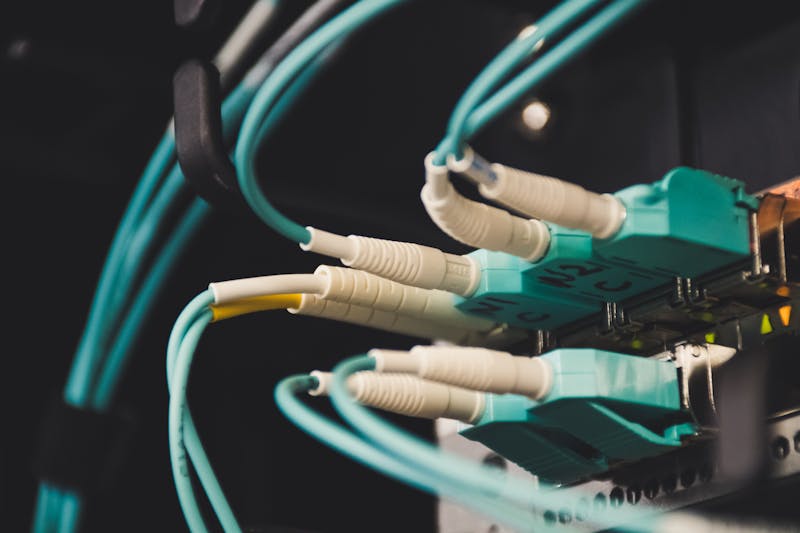
Nokia has signed a deal to take over NXP Semiconductors' fab in Chandler, Arizona, and convert it into a production site for indium phosphide (InP) optical chips — the components that carry traffic inside AI data centers. The Finnish telecom equipment maker will lease part of the facility from early 2027, then buy the full site, with the transaction expected to close in the first quarter of 2029, pending regulatory approval.
The acquisition, first reported by Semiconductor Today, gives Nokia a second US-based InP wafer fab, adding to the San Jose, California, plant it picked up through the Infinera acquisition in 2025. NXP had planned to shutter the Chandler campus in 2027 after the RF gallium nitride (GaN) business it supported lost momentum, so the site would have gone dark without a buyer.
Why Chips That Make Light Became the Hottest Shortage in AI
Indium phosphide is a III-V compound semiconductor — a marriage of two elements from columns III and V of the periodic table. Silicon can switch electrons around, but it cannot emit light efficiently. InP can. That property puts it at the heart of every laser inside an optical transceiver, the device that converts electrical signals to light pulses and back again at the ends of a fiber link.
The optics market has boomed because AI training clusters have outgrown copper. Nvidia's latest GPU racks, built around NVLink and 1.6T optical modules, push tens of terabytes per second between accelerators, and no electrical cable sustains that over distance. Every one of those links needs lasers, and nearly all of them start life on InP wafers.
The Shortage Behind the Deal
The supply picture is tight, and it is tightening. Lumentum CEO Michael Hurlston warned in early August that the supply-demand gap for InP has now surpassed that of DRAM and NAND, making it one of the most critical constraints on AI data center optical interconnect expansion. Lumentum runs several InP wafer fabs of its own and still cannot keep up: orders once counted in the hundreds for telecom customers have jumped to hundreds of millions of devices, driven by Nvidia and hyperscale data center operators.
The transition to 800G and 1.6T optical modules is the trigger. Each faster module consumes more InP substrate and epitaxial wafer material than the generation it replaces, while global capacity has not kept pace. Customers are placing orders further in advance and putting down substantial deposits to lock supply, inventories are tightening, and prices are rising.
There are structural reasons supply cannot snap back quickly. Indium is mostly recovered as a by-product of zinc refining, so output does not respond to chip demand alone. China produces roughly 70 percent of the world's refined indium and has tightened export controls on InP and indium since 2025, adding geopolitical risk to an already strained market. Making large-diameter InP substrates requires highly sophisticated crystal-growth technology, and yield improvements take years, not quarters. Production is also concentrated among a handful of suppliers, which limits how fast anyone can add capacity.
Why Nokia Wants to Make Its Own Optics
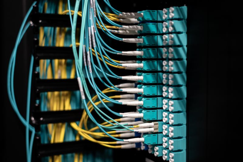
The purchase continues a strategy Nokia set in motion when it bought Infinera in early 2025. That deal brought a vertically integrated optical business: an InP wafer fab in San Jose and a back-end packaging and test facility in Pennsylvania. Nokia said it remains on track to begin ramping production at the San Jose fab in the fourth quarter of 2026, and during the second quarter it announced a tenfold increase in test and packaging capacity at the Pennsylvania plant, starting in the third quarter.
Chandler adds scale and a second US location. The fab opened in September 2020 and was once billed as the world's most advanced facility of its kind. Nokia said the site brings an experienced team with deep industry expertise in compound semiconductors, plus US-based InP manufacturing capacity at a time when secure and scalable domestic supply matters more to the broader US technology ecosystem and the AI data-center build-out. Bits&Chips noted the Chandler facility was heralded as the world's most advanced fab of its kind when it opened in 2020, and its shift from 5G power amplifiers to AI optics is a case study in how fast the industry's center of gravity has moved.
The move also sits inside a wider consolidation pattern. Hyperscalers and equipment vendors alike are deciding that optical components are too strategic to leave entirely to merchant suppliers. Nvidia has committed billions directly to InP upstream producers — in March 2026 it promised $2 billion to each of two key suppliers and signed long-term supply agreements. One of those suppliers has already doubled its 6-inch wafer capacity and plans another expansion by the end of 2027; the other is upgrading its 6-inch production line, with mass production expected in 2028. A leading Japanese supplier has also announced a multi-year expansion program. Industry analysts still expect the supply imbalance to persist beyond 2027.
What This Means for the AI Supply Chain
Optical interconnects are becoming a bottleneck category of their own, and this week's news cycle keeps reinforcing it. A new CIC forecast projects the data center optical interconnect market will grow from $13.7 billion in 2024 to $144.4 billion by 2030 — a tenfold jump in six years. Alongside Nokia's Chandler purchase, Applied Materials reported that advanced packaging and DRAM are accelerating its growth, and Veeco has announced more than $250 million in equipment orders for InP laser manufacturing.
For AI builders, the takeaway is blunt: the industry's next shortage may not be GPUs or memory, but the unglamorous laser chip that moves data between them. Nokia's bet is that owning the fab beats renting the supply chain, especially when a single material — indium phosphide — decides whether a data center can actually light up its racks.
An Old Fab Gets a Second Life
The Chandler site has had a short, bumpy history. Conceived when 5G build-outs were booming, it was built to make GaN power amplifiers for cellular base stations. Operator spending collapsed and 5G rollouts shrank, and NXP announced its exit from the 5G radio power market last December, with the fab slated for closure in 2027. Nokia's plan gives the building, its tools, and its roughly 700-person workforce a new mission in AI optics instead of a shutdown.
Regulatory approvals still stand between the deal and the handover. Nokia will start as a tenant in part of the facility in early 2027, which lets it begin qualifying production lines before the full acquisition closes in 2029. The phased structure de-risks the transition and gives customers a visible roadmap for US-made InP components.
The deal is the latest sign that semiconductor manufacturing is no longer only about silicon. Compound semiconductors — InP for optics, GaN for power, silicon carbide for EVs — are pulling their own fabs, their own supply chains, and their own billion-dollar investments as AI infrastructure scales. Nokia's Arizona bet is one of the clearest examples yet of a company deciding that the light inside the cable deserves a factory of its own.
More semiconductor industry coverage · AI infrastructure news · Data center and cloud computing