The US Department of Commerce is pouring $874 million into seven companies for next-generation semiconductor research and development, with GlobalFoundries landing the biggest single award at $300 million to develop silicon photonics technology that swaps copper wires for light-based data links inside AI data centers.
The awards, announced July 29, come as the SEMI industry group reported global silicon wafer shipments jumped 7.4 percent year-on-year in the second quarter of 2026, hitting 3,573 million square inches. The twin signals — government investment and sustained demand growth — point to a semiconductor sector that isnt slowing down, even after months of Wall Street jitters over AI spending.
GlobalFoundries signed a letter of intent with the Commerce Departments CHIPS Research and Development Office for $300 million to accelerate work on silicon photonics, a technology that uses light rather than electrical signals to move data between chips. The company says it targets data transfer speeds of 400 gigabits per second and a fivefold improvement in energy efficiency over todays pluggable optical modules.
Semiconductor Manufacturing Powers AI Data Centers
The shift is essential because AI clusters are hitting a wall. As Nvidia packs more compute into each rack and AMD strings together thousands of GPUs, the copper traces that link chips — even short ones inside a server — cant keep up. They consume too much power, generate too much heat, and bottleneck data at the worst possible moment: when a trillion-parameter model is trying to load.
"The bottleneck in AI infrastructure is shifting from compute to connectivity, the ability to move data between and within systems without letting bandwidth or power constraints limit performance," said Chris Koopmans, president and COO of Marvell, which builds networking chips that depend on optical links.
Photonics goes to the foundry
Silicon photonics isnt a new idea — researchers have worked on it for decades. What changed is that the physics now pencils out for volume manufacturing. GlobalFoundries has spent more than a decade building the platform and claims its ready to scale co-packaged optics (CPO), where a tiny laser and photonic integrated circuit sit right next to an AI processor inside the same package, slashing the distance data travels.
The funding will support work at GFs facilities in Malta, New York, and Burlington, Vermont. The company recently introduced its SCALE platform, which stands for Silicon Photonics Co-Packaged Advanced Light Engine, targeting modular designs that customers can customize without redesigning the entire optical link.
"This is essential to AI infrastructure," said Tim Breen, CEO of GlobalFoundries. "For a decade, the industry talked about the shift from copper to optical as something that was coming. Today it is here, moving data at higher bandwidth and improved power efficiency as workloads grow more complex."
AMD, Broadcom, Cisco, Corning, Lumentum, Marvell, Meta, Microsoft, Nvidia, and Qualcomm all issued statements of support for the GlobalFoundries initiative, signaling that the silicon photonics ecosystem has reached critical mass. AMD CTO Mark Papermaster called efficient data movement "as critical as increasing compute performance," while Nvidia founder Jensen Huang said "rebuilding our supply chains is critical to the new industrial revolution."
Seven R&D bets at once
GlobalFoundries wasnt the only winner. The Commerce Department signed letters of intent with seven companies totaling $874 million across a range of semiconductor R&D projects including integrated photonics, novel compute architectures, advanced packaging, substrates, novel materials, and new memory technologies.
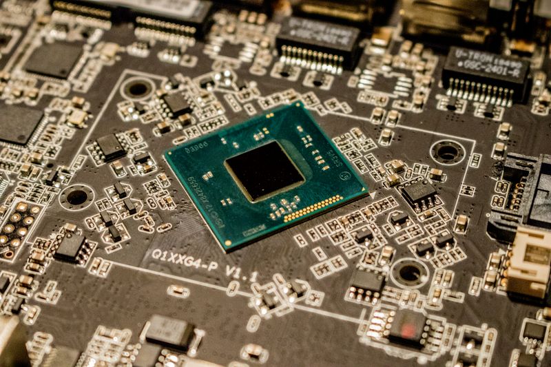
Kepler, which is listed among the recipients, is receiving up to $245 million for R&D to develop a new class of high-performance AI memory technology. The broader program targets the compute supply chain — the entire stack from raw silicon wafers through chip design, fabrication, packaging, and system integration — which the administration views as a strategic vulnerability given that much of the worlds advanced packaging and photonics capacity sits outside the United States.
"With todays compute supply chain investments, the Trump Administration is accelerating Americas innovation engine," said Secretary of Commerce Howard Lutnick. "These strategic investments will enhance our countrys domestic capabilities, create high-paying jobs and keep America at the forefront of the semiconductor industry."
The Department will take a minority, non-controlling equity stake in each company receiving funds, giving taxpayers a share in the upside.
Wafer shipments tell the real story
While policy announcements grab headlines, the SEMI wafer shipment data released the same day shows the industrys underlying momentum. Silicon wafer shipments — the fundamental building material for nearly every semiconductor — grew 9.1 percent quarter-over-quarter and 7.4 percent year-on-year in Q2 2026, reaching 3,573 million square inches.
"Wafer shipments maintained steady growth in the second quarter, driven by strong and increasing AI-related demand beyond advanced logic and memory to include power devices, photonics, and other markets," said Ginji Yada, chairman of the SEMI Silicon Manufacturers Group and an executive at SUMCO Corporation, one of the worlds largest silicon wafer producers.
He added that industrial and automotive demand is showing signs of recovery, though memory price pressures continue to constrain PC and smartphone demand. Device manufacturers are investing heavily in capacity expansion, and wafer demand growth is expected to continue through the second half of 2026.
The silicon wafer numbers matter because theyre a leading indicator for the broader semiconductor cycle. When fabs order more bare wafers from suppliers like SUMCO, Shin-Etsu, and GlobalWafers, it signals confidence that chip demand will be there six to nine months later — the typical fab cycle time. The Q2 numbers say the industry is loading up for a busy 2027.
The race for onshore capacity
The $874 million CHIPS R&D push and the GlobalFoundries award are part of a broader national strategy to bring semiconductor manufacturing back to American soil. Earlier this year, TSMC committed an additional $100 billion to its Arizona complex — bringing total investment to $265 billion — for 2-nanometer wafer fabrication. Intel has been scaling its advanced packaging operations in New Mexico, using technologies like Foveros stacking and EMIB interconnects to bypass the reticle limit and produce packages over eight times larger than industry standard.
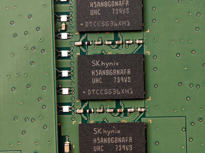
The GlobalFoundries award draws a direct line between R&D and onshore manufacturing. The company already runs fabs in Malta, New York (its 300mm Fab 8 complex) and Burlington, Vermont (Fab 9, which focuses on silicon photonics and specialty technologies). Unlike TSMCs race to the smallest transistor, GF competes on differentiated technologies — silicon photonics, RF-SOI, FD-SOI, power GaN — that serve markets where bleeding-edge density matters less than integration and energy efficiency.
Silicon photonics is the textbook example. The technology requires fab capacity that can handle optical waveguides, germanium photodetectors, and hybrid bonding alongside conventional CMOS transistors. GFs existing New York and Vermont lines already support these processes, giving the company a head start over pure-play logic foundries that would need to retrofit entire fabrication bays.
Whats next
The Commerce Department said the letters of intent are the first step. Final awards require further diligence and approval, with the CHIPS R&D Office continuing to solicit proposals for microelectronics research. For GlobalFoundries, the $300 million award covers next-generation optical materials, wafer technologies, and advanced packaging including 3D hybrid bonding.
"This builds on our already qualified portfolio of photonic devices, proven 3D hybrid bonding, and advanced packaging expertise," said Gregg Bartlett, GFs chief technology officer. "Were putting our customers on a direct, US-based path to scaling optical connectivity for tomorrows AI systems."
The immediate test is whether the industry can convert government R&D funding into production-scale silicon photonics modules within two to three years — the typical timeline the AI data center buildout demands. With Marvell, Broadcom, Cisco, and Nvidia all signaling they will design around GFs SCALE platform and the emerging CPO standard, the market pull is there. The question is whether the foundry can keep up with demand. For an industry that just posted 7.4 percent wafer shipment growth on AI alone, that is a nice problem to have.
The silicon photonics push comes at a moment when the entire semiconductor supply chain is being re-evaluated. Geopolitical tensions between the US and China have made onshore manufacturing a national security priority, not just an economic one. The CHIPS Act, signed into law in 2022, has already unlocked billions in private investment — TSMC alone has committed $265 billion to its Arizona complex, and Intel is spending heavily on its Ohio and New Mexico fabs. But the R&D piece had lagged behind the manufacturing incentives. The July 29 awards close that gap, pouring hundreds of millions into the kind of blue-sky research that foundries typically underinvest in because the payoff is five to ten years out.
For readers tracking the global race, the key number isnt $874 million or even $300 million — its the 7.4 percent wafer shipment growth, because that number, reported every quarter by SEMI, tells you whether the billions in government subsidies are getting spent on actual hardware or just sitting as budget line items. Right now, the wafers are moving. The task for GlobalFoundries, Kepler, and the other CHIPS R&D recipients is to turn that momentum into the next generation of optical interconnects, memory architectures, and packaging technologies that will keep Americas semiconductor industry competitive through the 2030s.