AI Reshapes the Semiconductor Landscape: Siemens-TSMC Partner on Design Automation, ON Semi Targets $213B Power Opportunity, and TSMC Hikes Wafer Prices
Introduction
September 2026 has delivered a concentrated wave of developments across the semiconductor industry that underscores the sector's accelerating pivot toward artificial intelligence workloads. Siemens and TSMC announced a collaboration on AI-powered semiconductor design automation, ON Semiconductor unveiled a strategy targeting a $213 billion AI power delivery opportunity, TSMC reportedly plans to raise wafer foundry prices amid tight advanced-node capacity, and Nexstrom closed a $12 million funding round to scale 2D semiconductor platforms for next-generation electronics. These developments, arriving within a 48-hour window, paint a picture of an industry in rapid transition: AI is no longer just a downstream consumer of chips but is fundamentally reshaping how chips are designed, manufactured, powered, and priced.
Siemens and TSMC Advance AI-Powered Design Automation
The Siemens-TSMC partnership, announced on September 23, represents one of the most consequential moves in the electronic design automation space in recent memory. The collaboration aims to embed artificial intelligence directly into the semiconductor design workflow, addressing one of the industry's most persistent bottlenecks: the increasing complexity of designing chips at advanced process nodes.
As transistors shrink below 3 nanometers, the number of possible design configurations explodes exponentially. Traditional design automation tools rely heavily on human engineers to make critical architectural decisions, optimize layouts for performance and power consumption, and verify that complex multi-billion-transistor designs function correctly before committing them to expensive fabrication runs. By integrating AI into this process, Siemens and TSMC aim to dramatically compress design cycles while improving the quality of silicon.
The partnership builds on Siemens' position as the dominant provider of electronic design automation software through its Mentor Graphics division and TSMC's role as the world's largest dedicated semiconductor foundry. The practical implication is that chip designers working with TSMC's advanced nodes will gain access to AI-assisted tools that can explore design spaces more efficiently, identify optimal placement and routing configurations, and predict manufacturing yield issues before tape-out. For the broader industry, the announcement signals that the AI transformation is not limited to the chips themselves but is reaching deep into the infrastructure that creates them.
The timing is significant. As AI chip demand continues to surge, foundries are under pressure to deliver more complex designs on shorter timelines. TSMC's N3 and N2 process nodes, along with the upcoming A16 backside power delivery technology, present design challenges that push human cognitive limits. AI-augmented design automation could prove to be the enabling technology that allows the industry to continue its path along Moore's Law trajectories even as traditional scaling approaches become increasingly difficult.
ON Semiconductor's $213 Billion AI Power Opportunity
ON Semiconductor's strategic presentation on the same day outlined the company's vision for capturing a share of what it estimates to be a $213 billion addressable market in AI power delivery. The figure is striking not for its size but for what it represents: the semiconductor industry's recognition that power management is becoming as critical as compute performance in the AI era.
The core insight driving ON Semiconductor's strategy is that AI workloads impose fundamentally different power delivery requirements than traditional computing. Modern AI accelerators, particularly large-scale training GPUs and inference ASICs, consume hundreds of watts per chip and operate at voltage levels that demand precision power regulation. The power delivery network that supplies clean, stable voltage to an AI accelerator operating at 700 watts has more in common with industrial power systems than with the VRM circuits that power a consumer desktop processor.
ON Semiconductor's power semiconductor portfolio — spanning silicon carbide MOSFETs, gallium nitride transistors, and silicon-based power management ICs — positions the company across the full spectrum of AI power delivery needs. The company's emphasis on silicon carbide and gallium nitride wide-bandgap semiconductors is particularly relevant as data centers increasingly operate at 48-volt power distribution architectures that require efficient DC-DC conversion at the rack and board level.
The $213 billion addressable market figure encompasses power semiconductors for AI training clusters, inference accelerators at the edge, power supply units for AI servers, and the power management circuitry integrated into the chips themselves. For investors and industry analysts, the number quantifies what has been an emerging narrative: that power delivery infrastructure is the constraint that will determine how quickly AI compute capacity can scale. The implication for ON Semiconductor is clear — the company is repositioning itself from a general-purpose power semiconductor supplier to an AI infrastructure specialist.
TSMC Raises Wafer Foundry Prices
In a development that could reshape the economics of chip production across the industry, reports emerged that TSMC plans to raise prices for its wafer foundry services. The price increases, if confirmed, would affect multiple process nodes and reflect the combination of rising input costs, increasing manufacturing complexity, and sustained demand that has kept TSMC's advanced node capacity fully allocated.
The price hike is significant because TSMC's pricing serves as a benchmark for the entire semiconductor manufacturing ecosystem. When the world's largest foundry raises prices, the effects ripple through every layer of the semiconductor supply chain. Fabless chip designers face higher per-unit costs, which they must either absorb or pass on to their customers — ultimately affecting the pricing of everything from smartphones to data center servers.
The context for the price increase is multifaceted. TSMC has invested billions of dollars in new fabrication facilities in Arizona, Japan, and Germany, and the capital expenditure required to bring these facilities online is substantial. The company's advanced nodes require increasingly expensive equipment, particularly extreme ultraviolet lithography systems from ASML, each of which costs hundreds of millions of dollars. Meanwhile, the growing power consumption of advanced fabs means that energy costs represent a significant and rising fraction of manufacturing expenses.
For customers, the price increase adds urgency to design optimization efforts. Every design improvement that increases yield or allows a chip to be manufactured on a less advanced (and less expensive) node becomes more valuable when wafer prices rise. This dynamic creates a feedback loop with the Siemens-TSMC AI design automation partnership: better AI-powered design tools can help optimize designs for cost efficiency, partially offsetting the impact of higher wafer prices.
Nexstrom's $12 Million for 2D Semiconductor Platforms
Nexstrom's $12 million funding round, announced in late September, brings attention to an emerging frontier in semiconductor materials: two-dimensional semiconductors. While traditional silicon chips continue to dominate production volumes, 2D materials such as molybdenum disulfide and other transition metal dichalcogenides offer properties that could be transformative for specific applications.
The key advantage of 2D semiconductors lies in their atomically thin structure, which allows for exceptional electrostatic control at extremely small dimensions. As silicon transistors shrink toward their physical limits, 2D materials offer a potential path forward for continuing to improve transistor performance and density. Nexstrom's focus on scaling 2D semiconductor production to 12-inch wafer platforms addresses one of the primary barriers to commercialization: the ability to manufacture these materials at volumes compatible with existing semiconductor fabrication infrastructure.
The investment reflects a broader trend in semiconductor research funding, where venture capital is flowing toward materials science innovations that could extend semiconductor performance trajectories beyond what silicon alone can achieve. While 2D semiconductors are unlikely to displace silicon in mainstream production within the next five years, the technology represents an important hedge against the possibility that traditional scaling approaches encounter insurmountable physical limits.
The AI-Driven Demand Surge for Memory
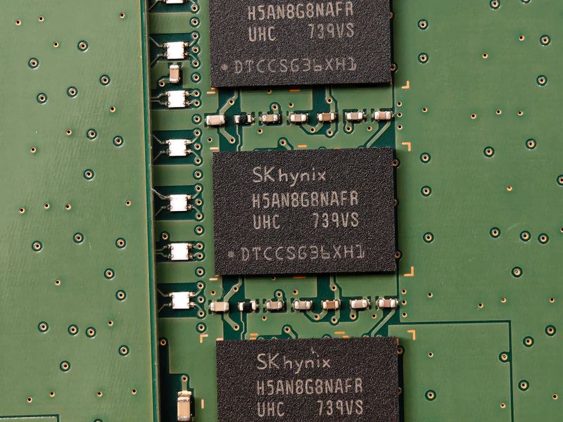
Separate market research published in the same timeframe projected that the semiconductor memory market will experience sustained strong growth through 2035, driven primarily by AI and high-bandwidth memory (HBM) demand. The projection reinforces the centrality of memory technology in the AI ecosystem and provides context for ongoing capacity investments at memory manufacturers including SK Hynix, Samsung, and Micron.
High-bandwidth memory, which stacks DRAM die vertically using through-silicon vias to provide the enormous memory bandwidth required by AI accelerators, has become the most strategically important segment of the memory market. NVIDIA's H100 and successor accelerators require multiple HBM stacks, and the growing size of AI models continues to push memory bandwidth requirements higher. The market research suggests that HBM demand will compound at a rate significantly above conventional DRAM growth, creating opportunities for manufacturers that can scale HBM production while maintaining the yield and reliability requirements demanded by AI chipmakers.
Michael Burry's Semiconductor Short
Adding a contrarian perspective to the bullish semiconductor narrative, investor Michael Burry disclosed short positions in Micron Technology and other semiconductor names. Burry's bearish stance on memory chips specifically suggests a thesis that the current cycle of capacity expansion in memory may lead to oversupply once the near-term AI demand surge moderates.
The contrast between Burry's short positions and the broader market's bullishness on semiconductor demand highlights a fundamental tension in the industry: the balance between near-term demand outstripping supply and the risk that massive capacity investments currently underway will create a cyclical glut when demand growth normalizes. For industry participants, Burry's position serves as a reminder that semiconductor markets remain inherently cyclical even as the secular demand trend points upward.
Conclusion
The September 2026 developments in the semiconductor industry collectively illustrate a sector undergoing simultaneous transformation on multiple fronts. AI is reshaping design tools, creating new power delivery requirements, driving memory demand to unprecedented levels, and influencing the pricing power of the world's most important foundry. The Siemens-TSMC partnership addresses the design complexity challenge, ON Semiconductor's $213 billion vision quantifies the power opportunity, TSMC's price increases reflect the economic realities of advanced manufacturing, and Nexstrom's funding round points toward materials science innovations that could extend semiconductor performance trajectories.
What emerges from these developments is an industry where the traditional boundaries between design, manufacturing, power delivery, and materials research are dissolving under the pressure of AI demand. The companies that thrive in this new landscape will be those that can integrate across these domains — leveraging AI to optimize designs, delivering efficient power solutions for AI workloads, and advancing materials science to sustain performance gains. The semiconductor industry of September 2026 is no longer just making chips for AI; it is fundamentally reinventing itself around the requirements of artificial intelligence.
Images

References
- Siemens and TSMC Advance AI-Powered Semiconductor Design Automation, Siemens Digital Industries, September 23, 2026
- Here's How ON Semiconductor Is Targeting a $213 Billion AI Power Opportunity, Yahoo Finance, September 23, 2026
- Semiconductor Memory Market To 2035: AI and HBM Demand Drive Forward Growth, IndexBox, September 24, 2026
- Nexstrom Raises $12M to Scale 12in Single-crystal 2D Semiconductor Platform, eetasia.com, September 23, 2026
- Michael Burry Shorts Micron, Palantir; Famed Investor Expects Chip 'Down Cycle', Investor's Business Daily, September 23, 2026
- The AI Factory Is Becoming the Computer and It's Changing the Semiconductor Race, SiliconANGLE, September 23, 2026
- Semiconductor